The Evolution of PCB Manufacturing: Trends and Innovations in 2024
In the fast-paced world of electronics, Printed Circuit Board (PCB) manufacturing has come a long way from its humble beginnings. As we move through 2024, PCB manufacturing is increasingly shaped by technological advancements that streamline production, enhance performance, and meet the demands of smaller, more powerful devices. Let’s dive into the current trends and innovations that are transforming PCB design, materials, and production technologies.
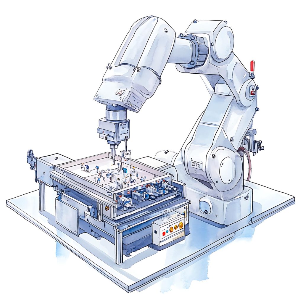
1. AI and Automation Revolutionizing PCB Production
Artificial Intelligence (AI) and automation are significantly transforming the PCB manufacturing landscape. By integrating AI with manufacturing processes, companies can now leverage predictive analytics, real-time monitoring, and automated decision-making to streamline production. AI-powered systems can identify defects early, optimize design layouts, and ensure better yield rates by minimizing human error.
Automation is also enhancing speed and precision in the PCB production process. For instance, automated placement machines, which position components onto the PCB, have become more accurate, faster, and capable of handling complex, high-density designs. These advancements help manufacturers meet the rising demand for miniaturized electronics without compromising quality.
2. Advanced PCB Materials for High-Performance Applications
In recent years, there has been a significant shift towards using advanced materials to meet the performance requirements of modern electronics. For example, high-frequency PCBs are now using materials like PTFE (Polytetrafluoroethylene) and ceramic-based substrates, which allow for faster signal transmission and better heat dissipation. These materials are ideal for applications in 5G, automotive electronics, and aerospace.
Moreover, the growing demand for flexible electronics has led to the rise of flexible and rigid-flex PCBs. These PCBs combine flexibility with durability, making them ideal for wearable devices, foldable smartphones, and medical implants. The ability to integrate such PCBs into compact, lightweight designs is fueling innovation across various industries.
3. The Rise of 5G and IoT: Impact on PCB Design
The rollout of 5G technology and the proliferation of IoT devices have a profound impact on PCB manufacturing. As these technologies demand higher data speeds and more reliable connectivity, PCBs need to be designed with greater precision and capacity. High-speed signals, reduced power consumption, and compact designs are now critical requirements for PCB manufacturers catering to 5G and IoT markets.
The integration of 5G into consumer and industrial devices necessitates the use of advanced PCB designs that can handle high-frequency signals with minimal signal loss. This shift is driving the development of microvias and laser-drilled holes for more compact routing paths and improved electrical performance.
4. Sustainability in PCB Manufacturing
As sustainability becomes a growing concern in the electronics industry, PCB manufacturers are adopting eco-friendly practices. The push for greener PCBs is driving innovation in materials and processes. For example, lead-free soldering and the use of recyclable materials are becoming standard practices to reduce environmental impact.
Additionally, efforts to reduce e-waste are leading to the development of biodegradable PCBs, which are being explored for certain low-end applications. These innovations aim to reduce the carbon footprint of the electronics industry while maintaining high levels of performance.
5. The Role of Advanced Fabrication Techniques
Advancements in fabrication techniques are enabling faster, more efficient production processes. Techniques like direct imaging and laser etching are replacing traditional photolithography methods, allowing for finer trace patterns and faster prototyping. These technologies enable manufacturers to produce more intricate and precise designs at a faster pace, driving down costs and enhancing efficiency.
Additionally, 3D printing is starting to gain traction in PCB prototyping. 3D printing enables the creation of complex, custom PCB designs with reduced lead times and lower costs. This technology is particularly beneficial for companies producing low-volume, high-mix products or for rapid prototyping in research and development environments.
6. Improved Testing and Quality Control
In 2024, PCB manufacturers are relying on more sophisticated testing and inspection systems to ensure the highest quality standards. Automated Optical Inspection (AOI), X-ray inspection, and electrical testing are commonly used to detect faults such as solder joint issues, component misplacements, and electrical shorts. These technologies improve the accuracy and reliability of PCBs, ensuring that only defect-free boards make it to the final product.
Furthermore, in-circuit testing (ICT) and functional testing are being employed to verify the operational performance of PCBs in real-world applications, reducing the risk of product failures in the field.
Conclusion
The evolution of PCB manufacturing in 2024 is being driven by advancements in AI, automation, materials, and fabrication technologies. As the electronics industry continues to push the boundaries of what’s possible with smaller, faster, and more efficient devices, PCB manufacturers must stay ahead of these trends to remain competitive. From the integration of AI for predictive analytics to the rise of flexible and sustainable materials, the future of PCB manufacturing promises to be as dynamic and innovative as the devices it supports.
By understanding and adopting these emerging trends, businesses can ensure they remain at the forefront of the rapidly changing world of electronics manufacturing.
Hey
I'm Emma!

Lorem ipsum dolor sit amet, consectetur adipiscing elit. Ut elit tellus, luctus nec ullamcorper mattis, pulvinar dapibus leo.