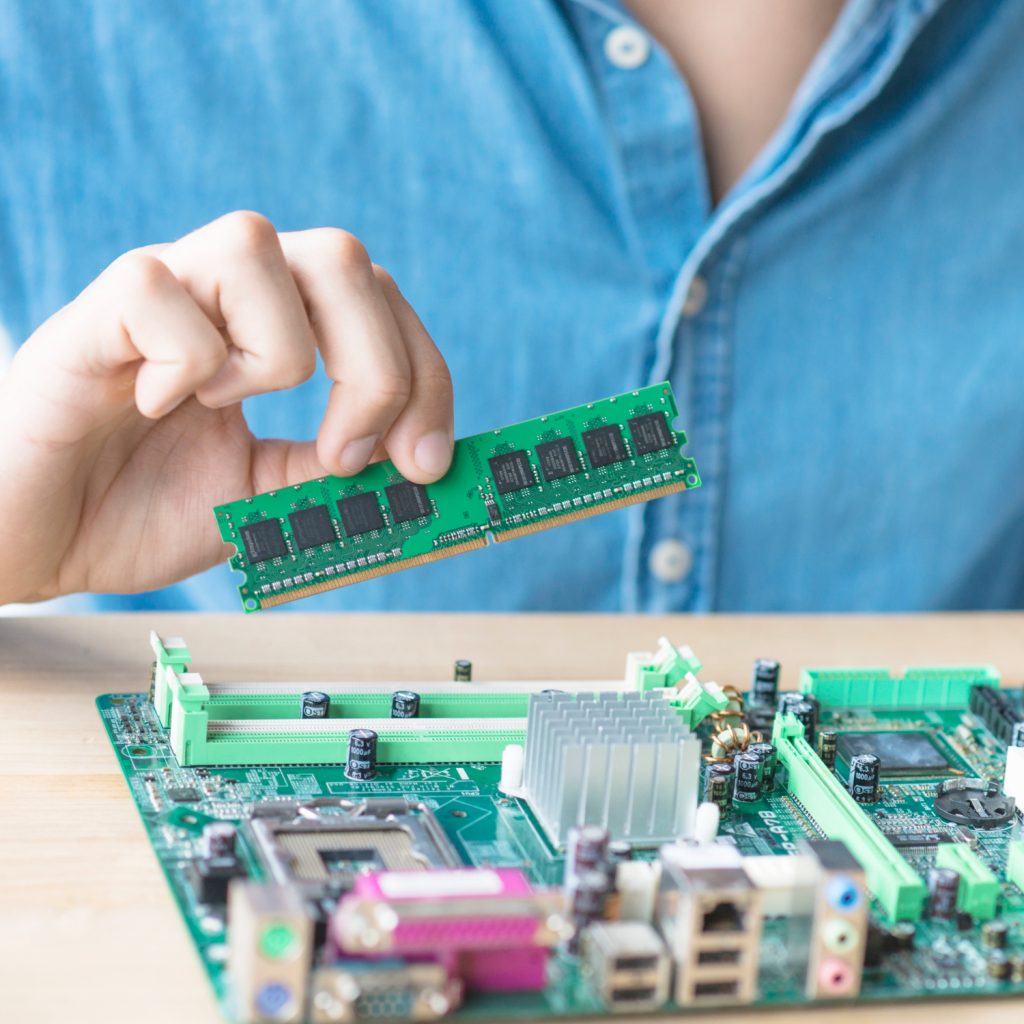
Best Practices for PCB Assembly Testing: Ensuring Quality and Functionality
In the world of PCB assembly, ensuring the quality and functionality of the finished product is paramount. Whether it’s for consumer electronics, automotive systems, or medical devices, a malfunctioning PCB can lead to failures, recalls, and costly repairs. To avoid these pitfalls, PCB testing is a crucial part of the manufacturing process. In this blog, we’ll explore the best practices for PCB assembly testing, covering techniques like electrical testing, visual inspection, and advanced methods like automated optical inspection (AOI) and X-ray testing.
1. Electrical Testing: The Foundation of PCB Testing
Electrical testing is one of the most fundamental methods to verify the functionality of a PCB. This process ensures that the electrical paths are correctly connected, and all components are functioning as intended. There are two main types of electrical testing used:
- In-Circuit Testing (ICT): This involves checking individual components and connections on the PCB using a bed-of-nails tester or similar setup. It allows for detailed analysis of resistances, capacitances, and continuities across the board. ICT is highly effective for detecting faults such as short circuits and open circuits in the components and traces.
- Functional Testing: Functional testing checks the PCB’s behavior in real-world conditions by simulating the operation of the device in its intended environment. It verifies that all components perform under expected loads and conditions, ensuring that the product will operate as intended once it reaches the market.
Sources:
- PCBWay discusses the importance of in-circuit testing for detecting faults at the component level.
- SMTnet elaborates on functional testing and how it provides a more comprehensive evaluation of a PCB’s operational capabilities.
2. Visual Inspection: A First Line of Defense
While electrical testing ensures the functional integrity of a PCB, visual inspection is an essential first line of defense against common defects that may affect the board’s performance. Visual inspection helps identify soldering issues, misalignment of components, and physical damage to the PCB such as cracks or scratches.
- Manual Inspection: Traditionally, technicians inspect boards manually under magnification, identifying problems like cold solder joints or misplaced components.
- Automated Optical Inspection (AOI): AOI systems use high-resolution cameras to inspect the board at various stages of assembly. This automated inspection helps detect soldering defects, component misplacement, and alignment issues that can be difficult for the human eye to catch. With the added benefit of machine learning, modern AOI systems are becoming increasingly accurate at identifying anomalies in PCB designs.
Sources:
- The IPC provides guidelines for using visual inspection and AOI techniques effectively in the PCB assembly process.
- According to Test & Measurement World, AOI systems are crucial for early detection of issues, minimizing defects in high-volume production.
3. X-Ray Testing: Detecting Hidden Defects
As PCBs become more complex and the components smaller, traditional inspection methods may not be enough. X-ray testing is used to reveal hidden defects, particularly in ball grid array (BGA) components where solder joints are not visible to the naked eye. X-rays can inspect the inner layers of a PCB, identifying issues such as voids, insufficient solder, and bridging that might go unnoticed in visual inspections.
- Micro X-ray Inspection: This technique allows for in-depth analysis of BGAs and CSPs (Chip-on-Board Surface Mount) where the solder joints are hidden beneath the component. It provides high-resolution images of the internal structure, allowing manufacturers to detect imperfections that could compromise the device’s reliability.
Sources:
- PCBTech outlines the use of X-ray inspection in advanced PCB assemblies for detecting hidden solder defects, especially in high-density packages.
- EETimes discusses how X-ray testing is integral for detecting hidden defects in PCBs with fine-pitch components.
4. Automated Optical Inspection (AOI): Enhancing Precision and Efficiency
Automated Optical Inspection (AOI) is rapidly becoming an industry standard due to its ability to quickly and accurately detect defects in PCB assemblies. By using high-resolution cameras and image processing software, AOI systems can identify a wide range of issues, including misplaced components, incorrectly placed solder pads, and damaged tracks.
- Pre-Reflow AOI: This is typically performed before the PCB enters the solder reflow oven, enabling early identification of placement errors that could cause failure during soldering.
- Post-Reflow AOI: After soldering, AOI verifies that the soldering quality is up to standard, ensuring cold joints and solder bridges are minimized.
Sources:
- Techopedia emphasizes how AOI systems increase the speed and accuracy of the inspection process, offering a detailed view of soldering quality.
- SMT Online points out how AOI minimizes human error and speeds up PCB assembly, making it an essential part of modern manufacturing lines.
5. Best Practices for PCB Assembly Testing
To ensure the highest quality and functionality in your PCB assembly, here are some best practices:
- Early Detection: Integrating testing early in the assembly process can catch defects before they propagate. Use pre-reflow and post-reflow AOI to address errors at the earliest stages.
- Comprehensive Testing: Combine electrical testing, visual inspection, AOI, and X-ray testing to ensure all aspects of the PCB are thoroughly tested.
- Regular Calibration: Keep inspection and testing equipment properly calibrated to ensure accurate and reliable results.
- Automate Where Possible: Utilize automation to increase testing speed and consistency, reducing human error and increasing throughput.
Conclusion
Testing is an integral part of the PCB assembly process that ensures a high-quality and functional final product. From basic electrical testing to advanced AOI and X-ray inspection, manufacturers must adopt a range of testing techniques to detect and correct defects at every stage of the assembly process. By following best practices and leveraging modern technologies, companies can produce reliable PCBs that meet the rigorous demands of today’s fast-paced electronics market.
By implementing robust testing strategies, PCB manufacturers can avoid costly mistakes and ensure that their products meet the highest quality standards, guaranteeing performance and reliability for end users across various industries.
Hey
I'm Emma!

Lorem ipsum dolor sit amet, consectetur adipiscing elit. Ut elit tellus, luctus nec ullamcorper mattis, pulvinar dapibus leo.
