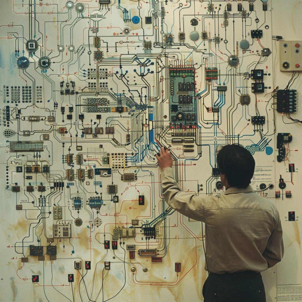
Challenges in PCB Manufacturing and How to Overcome Them
Printed Circuit Board (PCB) manufacturing is a complex process that requires precision, accuracy, and a deep understanding of materials, design, and assembly techniques. However, there are several challenges that manufacturers often face during PCB fabrication and assembly. These challenges can impact product performance, increase production costs, and cause delays in delivery. Let’s explore some of the most common issues encountered in PCB manufacturing and discuss effective strategies to overcome them.
1. Yield Issues
Yield issues occur when a batch of PCBs does not meet the required specifications, resulting in lower-quality products and higher costs. This problem is usually tied to issues in the fabrication process, including problems with the etching process, component placement, or soldering.
How to Overcome Yield Issues:
- Enhanced Process Control: Implementing more stringent controls during each stage of the manufacturing process can help minimize errors. Advanced tools like Automated Optical Inspection (AOI) and X-ray inspection can detect faults early, allowing for correction before the process moves forward.
- Regular Equipment Maintenance: Well-maintained equipment ensures that the processes, such as etching and soldering, are consistent. Routine checks and calibration can prevent issues that lead to yield loss.
- Design Optimization: Working with design engineers to ensure the design files are optimized for manufacturing (DFM – Design for Manufacturability) can reduce errors in the production process.
2. Component Misplacement and Soldering Issues
Component misplacement is a frequent problem that occurs during the pick-and-place process, where the components are not properly aligned or positioned on the PCB. Similarly, soldering defects such as cold solder joints, solder bridges, and insufficient solder can lead to poor performance or failure of the PCB.
How to Overcome Component Misplacement and Soldering Issues:
- Automated Pick-and-Place Machines: Using high-precision pick-and-place machines can greatly reduce human error in the component placement process. These machines are capable of placing components accurately and consistently, minimizing misplacement issues.
- Advanced Soldering Techniques: Techniques like wave soldering, reflow soldering, and selective soldering can be employed to ensure the soldering process is precise. Additionally, visual inspections and X-ray inspection are effective in identifying any soldering defects.
- Component Verification: Verifying component placement with Automated Optical Inspection (AOI) before soldering helps ensure that components are correctly placed and oriented.
3. Testing Challenges
Testing PCBs is one of the most crucial steps in the manufacturing process. However, it can be fraught with difficulties, such as identifying hidden faults or achieving consistency across multiple units. Faults in the PCB may not always be visible, making testing even more challenging.
How to Overcome Testing Challenges:
- In-Circuit Testing (ICT): ICT is a highly effective way to detect faults in individual components, such as resistors, capacitors, and ICs, by checking their connections to the PCB. This type of testing can be performed quickly and at a high level of accuracy.
- Functional Testing: In addition to ICT, functional testing simulates real-world operating conditions to ensure that the PCB functions as intended. This helps identify issues that may arise during normal operation, which may not be evident in earlier stages of testing.
- Test Automation: Automating the testing process with specialized equipment and software can speed up testing while reducing human error. Automated testing systems can be integrated into the production line, providing continuous feedback and faster identification of defects.
4. PCB Warping and Delamination
Warping and delamination are common issues that arise during PCB fabrication, particularly when the materials are exposed to excessive heat or stress. Warping can affect the alignment of components, and delamination can lead to a loss of electrical integrity, both of which can result in product failure.
How to Overcome Warping and Delamination:
- Material Selection: Choosing the right base material is essential for minimizing warping and delamination. Using high-quality laminates like polyimide or ceramic PCBs can prevent these issues, as they have better resistance to heat and stress.
- Optimizing the Curing Process: The curing process in PCB manufacturing must be tightly controlled to prevent warping. Overheating or under-heating the PCB during the curing phase can lead to unwanted warping or delamination. Controlled cooling and temperature ramping are important to mitigate these issues.
- Proper Stack-up Design: The stack-up design, or how the PCB layers are arranged, should be optimized to reduce internal stress. Symmetry in layer thickness and balanced copper distribution can help prevent warping.
5. Environmental and Regulatory Compliance
PCB manufacturing is heavily regulated, with strict standards to ensure environmental sustainability and compliance with international laws. Manufacturers face challenges in meeting these regulations, such as restrictions on the use of hazardous materials (e.g., lead and cadmium) and ensuring that the manufacturing process does not harm the environment.
How to Overcome Environmental and Regulatory Challenges:
- Adopt Lead-Free Manufacturing: To comply with regulations like RoHS (Restriction of Hazardous Substances), PCB manufacturers should adopt lead-free soldering and use environmentally friendly materials. This not only ensures compliance but also reduces the environmental footprint of the manufacturing process.
- Sustainability Practices: Incorporating recycling programs, waste reduction techniques, and green chemistry practices into the PCB production process can help reduce environmental impacts and maintain compliance with regulatory standards.
- Stay Informed on Regulations: Manufacturers must stay up to date with evolving regulations. This includes understanding changes to environmental legislation, product safety standards, and quality control measures to avoid costly mistakes.
Conclusion
While PCB manufacturing comes with several challenges, there are numerous ways to overcome them. By embracing advanced technologies like automated machines, optimizing designs for manufacturability, and improving testing and inspection methods, manufacturers can improve their processes, reduce defects, and enhance product reliability. Additionally, paying attention to environmental sustainability and regulatory compliance ensures that PCB manufacturing can meet industry standards and contribute to a safer, greener future.
By proactively addressing these challenges, PCB manufacturers can improve the overall production cycle, ensuring high-quality products that meet customer demands in a timely and efficient manner.
Hey
I'm Emma!

Lorem ipsum dolor sit amet, consectetur adipiscing elit. Ut elit tellus, luctus nec ullamcorper mattis, pulvinar dapibus leo.